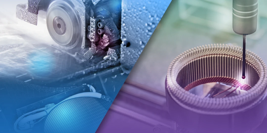
semiconductor manufacturing equipment and precision measuring systems.
Our philosophy is to generate long-term growth through the creation of "WIN-WIN,"
or mutually beneficial, relationships, with all our stakeholders - customers,
business partners, shareholders and lnvestors and employees.
Company information
Global Network
Tokyo Seimitsu Group
active around the world
Tokyo Seimitsu has bases in Japan
and other major regions of the world,
and leads the industry with world-class quality
in both its semiconductor production equipment
and precision measuring instrument businesses.

History of ACCRETECH
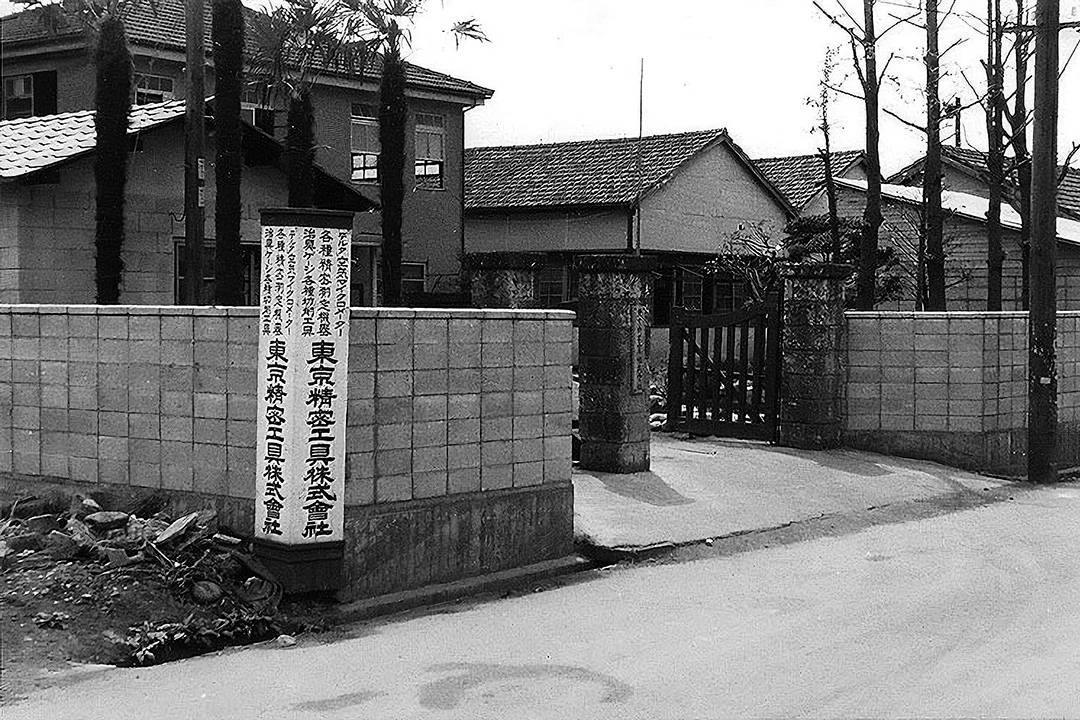
1949
Established Tokyo Seimitsu Kogu Co., Ltd.
We started out in the precision instrument business, and for more than 70 years since then, we have been refining our "ability to measure precisely" and creating new technologies and products for the world.
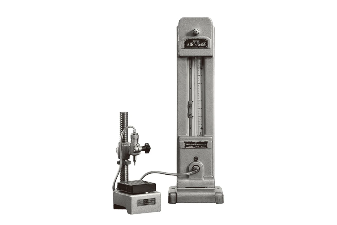
1952
Developed and commercialized Japan's first air micrometer
Japan’s precision industry began to develop, increasing needs for advanced instruments that could enable effective micron-level measurement regardless of changes in ambient conditions caused by dust, powder, temperature and other factors. The solution in those days was the air micrometer.
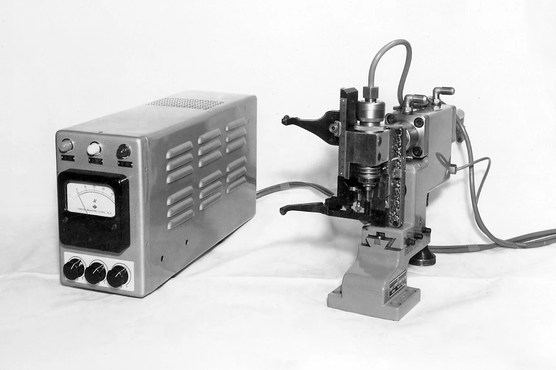
1957
Developed Palcom A, automatic positioning machine for cylindrical grinders
The automatic positioning machine was the first product to utilize an electric micrometer and was the first product diversification of Tokyo Seimitsu Kogu.
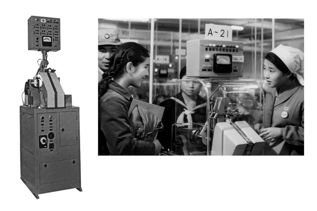
1958
Developed germanium pellet auto-sorter
The development of a fully automated sorting machine that fully automates the thickness measurement of fine parts to the micron level and enables grade sorting was the catalyst for Tokyo Seimitsu's entry into automated precision m achinery manufacturing for electronic components and semiconductor-related products.
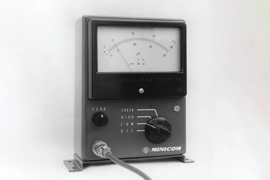
1961
Developed transistor type small micrometer
The use of transistors in this product has made the conventional tangerine box-sized electric micrometer into a lunch box-sized product with numerous advantages, including power savings. The rechargeable battery made it easy to carry around, which was especially revolutionary.
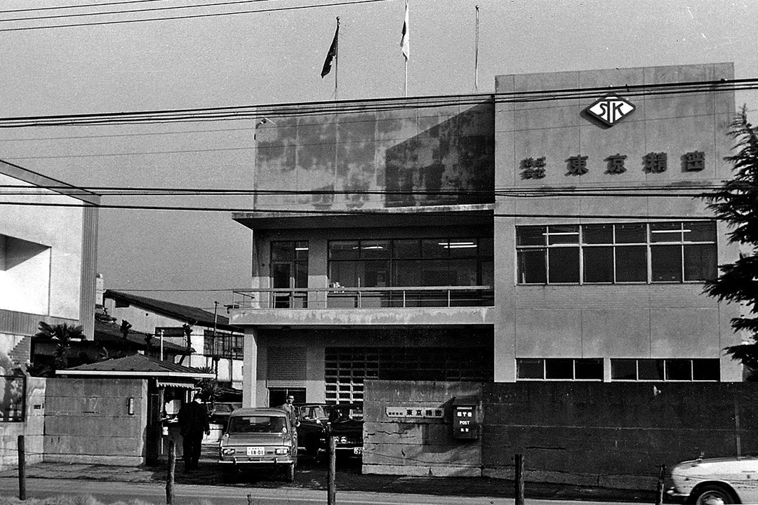
1962
Renamed Tokyo Seimitsu Co., Ltd.
Changed the company name removing "Kogu (Tools)" intending to express our commitment to expanding business areas.
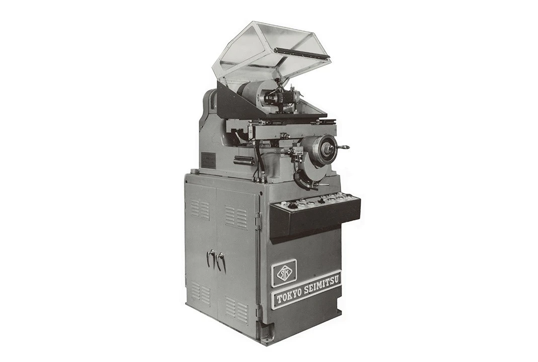
1963
Developing Japan’s first internal diameter blade-type slicing machine
While maintaining its traditional technical strength in precision measurement, the company promoted product development in other areas, with a particular focus on semiconductor-related products. Among those was the silicon wafer slicing machine, a descendent of the transistor performance auto-sorter. Around 1962, a project was launched to develop the internal diameter blade-type slicing machine. The relevant team s truggled to solve thorny problems with the design and production of spindles, setting internal diameter blade cutters, among others, before the project was completed successfully in February 1963.
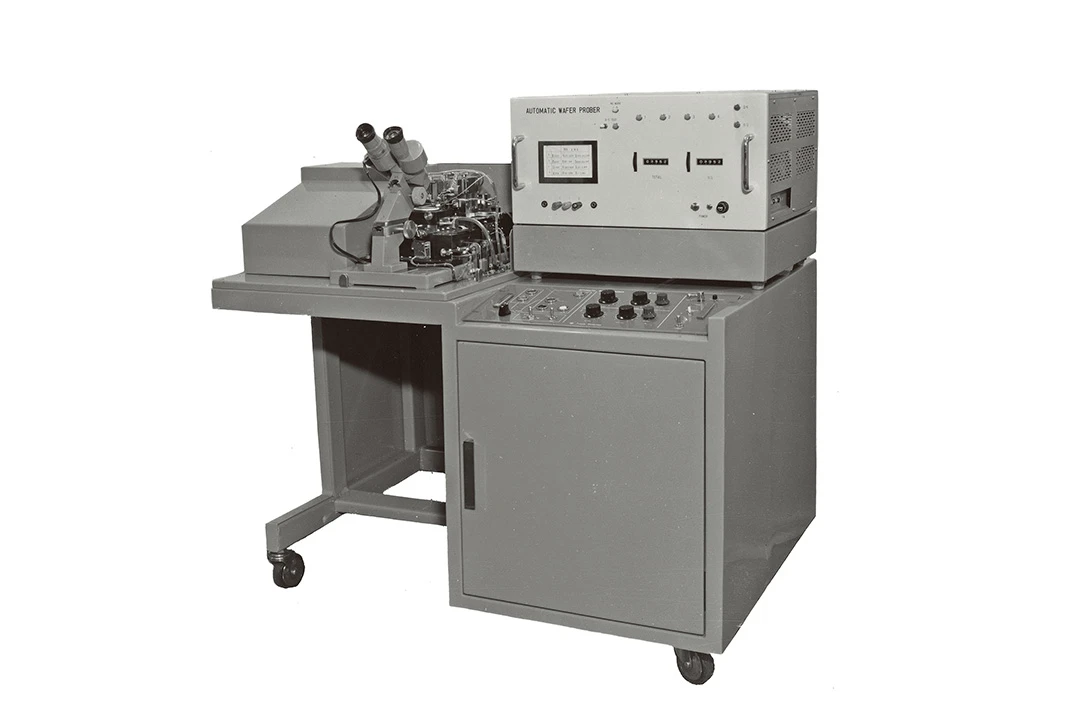
1964
Developed Japan's first probing machine
At that time, the probing machines were delivered to all semiconductor manufacturers in Japan. It is still one of the products that support the Company to this day.
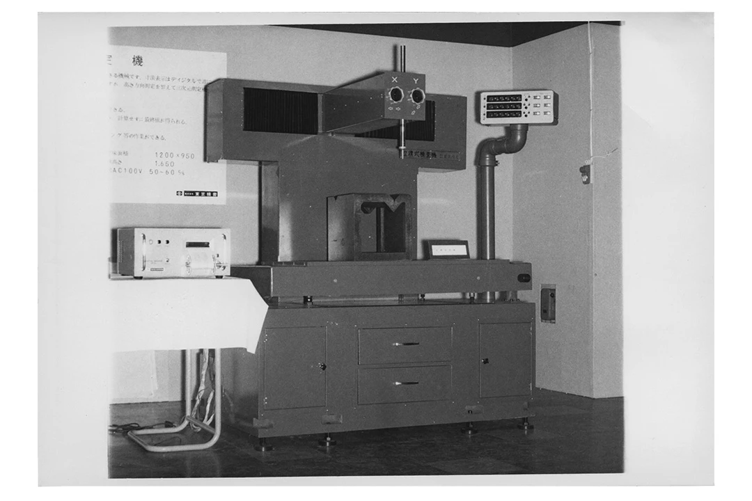
1969
Developed DCM-600A, Japan's first coordinate measuring machine
Behind its completion were the efforts of the engineering team to solve various technical issues.
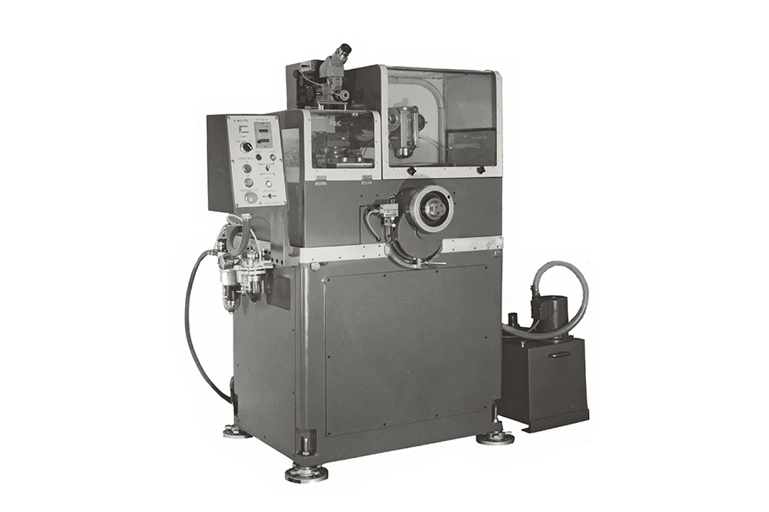
1970
Developed Japan's first wafer dicing machine
The machine's method of cutting with a thin blade rotating at high speed while water flows through the blade contributed to improved accuracy and efficiency in the chip-splitting process.
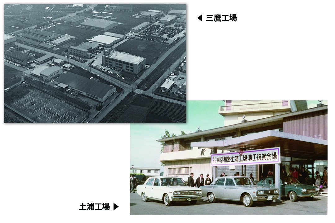
Tsuchiura Plant and Hachioji Plant completed
The plant facilities were complete with the completion of both plants and could enter full operation.
1979
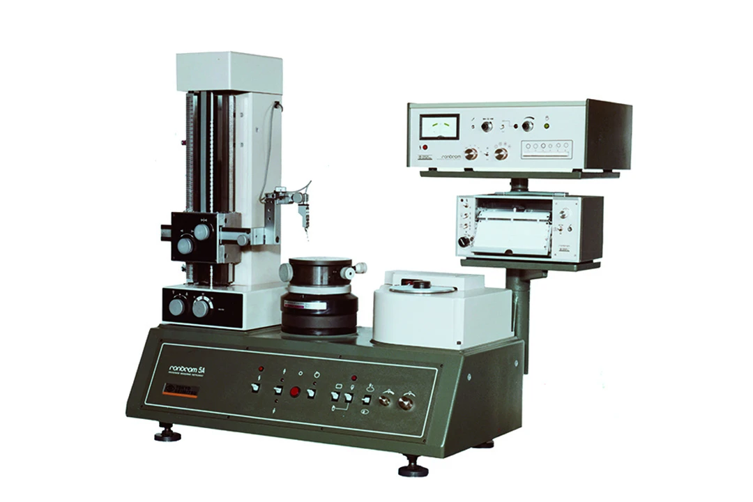
Developing RONDCOM 5A roundness and cylindrical profile measuring instrument
The RONDCOM 5A was released in 1979, looking to offer a definitive solution to high-accuracy cylindrical form analysis. It was equipped with ultra high-accuracy rotation air bearings boasting the then world’s highest level of performance. The instrument was highly rated for boosted functionality in accuracy, resistance to temperature changes and durability.
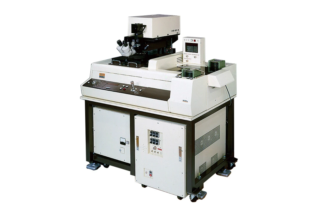
Japan's first fully automatic wafer probing machine
Developed Japan's first fully automated probing machine, the A-PM-3000A, which is compatible with 5-inch wafers in response to the needs of semiconductor manufacturers . The A-PM-3000A fully automates the entire process from loading to storing wafers, and only the first wafer is aligned by human touch, while the second wafer is aligned by laser beam. With the A-PM-3000A, we have established a foothold as the leading manufacturer of probing machines in Japan.
1980
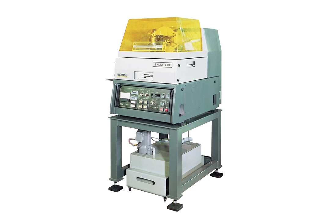
Developed S-LM-500, slicing machine
Commercialized two series of computerized internal diameter blade-type slicing machines?the S-LM-50E and S-LM-200?in 1980 and 1981, respectively. Introducing these series, we won a commanding share in the Japanese market, and carried out persistent marketing activities overseas to draw global attention. We continued developing this area to become the world’s top slicing machine manufacturer with a 70 to 80% share in the global market.
1981
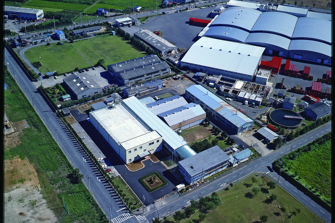
Opened plant for coordinate measuring machines at Tsuchiura Plant
Built a plant dedicated to coordinate measuring machines at the Tsuchiura Plant, which was completed in 1981. The plant was equipped with advanced and specialized development and production functions to produce a range of high-level machines. Among such products was the XYZAX PA-A, a CNC 3D coordinate measuring machine series commercialized in 1989, which boasted high-speed, high-accuracy and high-operability performance.
1984
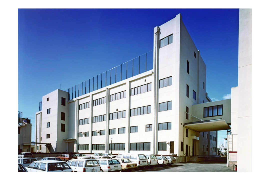
Factory No.1 at Hachioji Plant completed
A modern plant suitable for the production and development of semiconductor manufacturing equipment was constructed in the Hachioji area to increase production capacity.
1986
Listed on first section of Tokyo Stock Exchange
Received recognition as an excellent company in terms of both performance and finances, and made a great leap forward as an equipment manufacturer.
1990
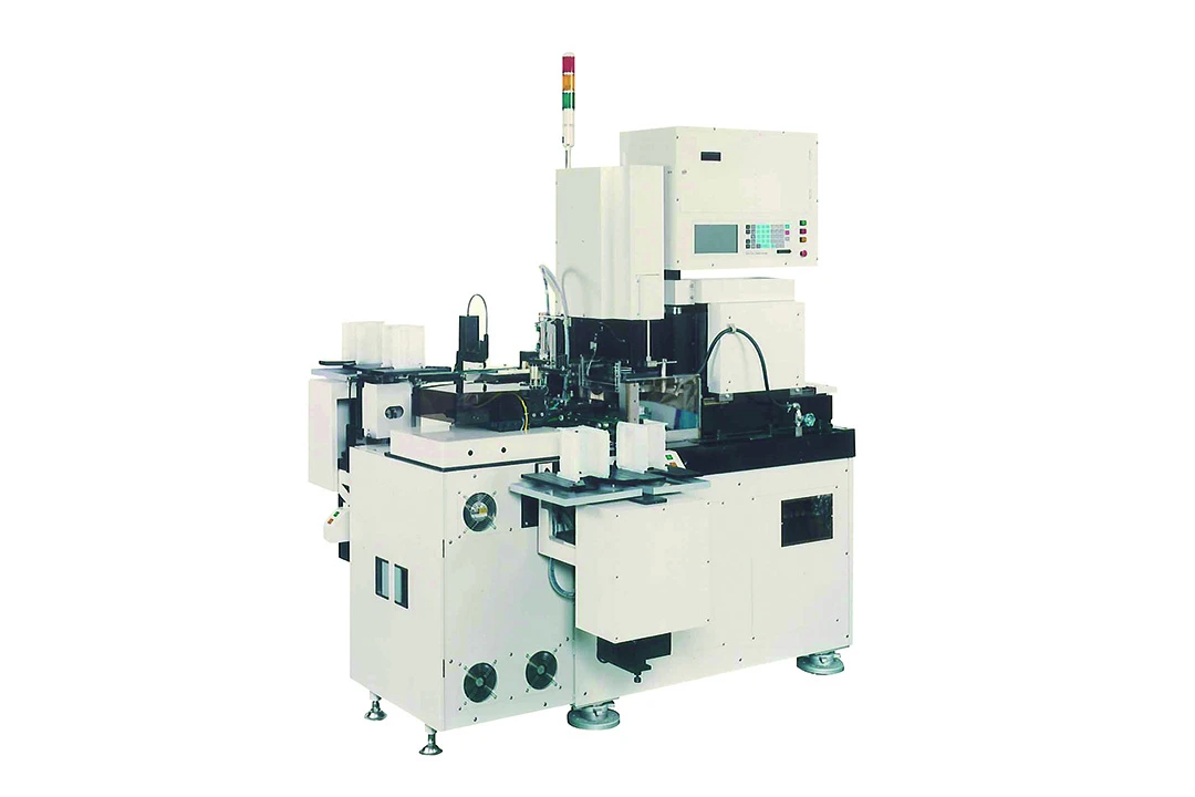
Developed Edge Grinding Machine
Wafers cut by slicing machines come into contact with wafer cassettes and guides during the process, which causes chipping and cracking on the outer edge of the wafer, resulting in a lower wafer yield. To eliminate this chipping and cracking, the W-GM-2000B edge grinding machine was developed to chamfer the wafer periphery.
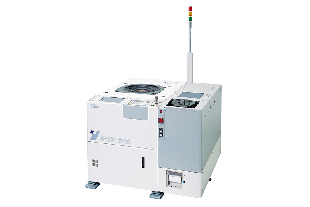
1992
Developing the A-PM-90A fully automatic wafer probing machine
The A-PM-90A, rolled out in 1992, boasted high specifications represented by “next generation, high precision, high operability, high reliability and high scalability.” The development was pursued under the Group Leader System with the aim of grabbing the top position in the global market. In addition to advanced product features, such as a 10-inch color LCD and touch panel control, strong sales and support functions were built to enhance relevant customer relations. As a result, the product garnered high praise from around the world, achieving enormous market success that helped the company become the world’s leading prober manufacturer in name and reality.
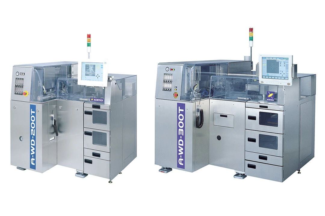
1999
Developed the world's first opposed two-axis wafer dicing machines
Successfully commercialized a fully-automatic blade dicing machine with opposed two-axis spindles, laying the foundation for the dicing industry.
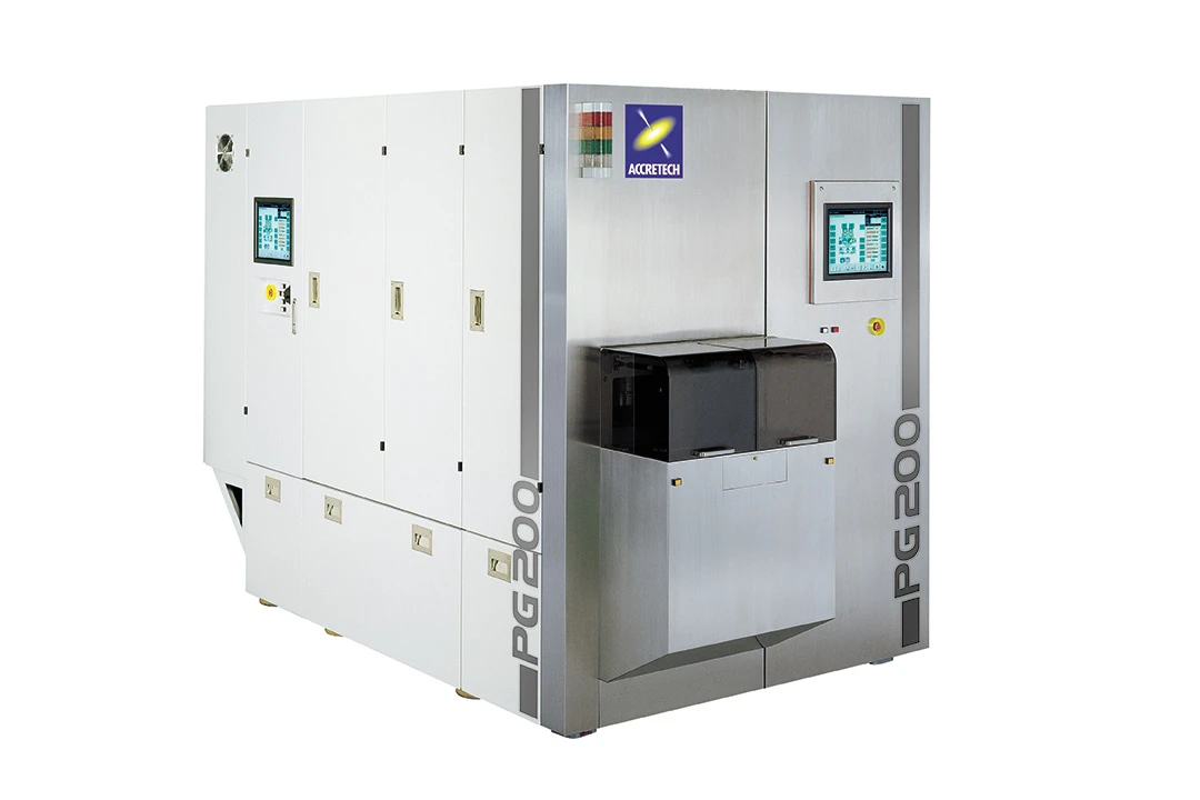
2000
Developed PG200, the world’s first polish grinder
This product, based on our original conception, enabled rough grinding, finish grinding, and polishing and cleaning processes while wafers were still held on the chuck table, thus enabling thinner wafers in a variety of products.

2001
Introduced the corporate brand ACCRETECH
Made a new start with the aim of becoming a global company that grows together with our stakeholders.
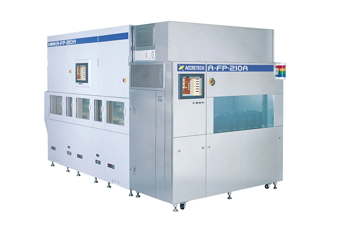
2002
Developed A-FP-210A (CMP)
The CMP (chemical mechanical planarizer) was designated as a priority product along with wafer inspection systems. This was directed at enhancing abilities to satisfy an industrial need for quality wafer surface polishing results, which was growing at the time as wafer diameters increased. Larger diameters require more complicated wiring, making the wafer surface more likely to suffer from irregularities, which must be eliminated through polishing and planarizing. Seeking to differentiate ourselves in the large and intensely competitive CMP market, we leveraged our technologies to develop a CMP that could deliver outstanding uniformity and stable polishing results through incorporating an air-float polishing head and a real-time end point detector that can support next-generation copper processing.
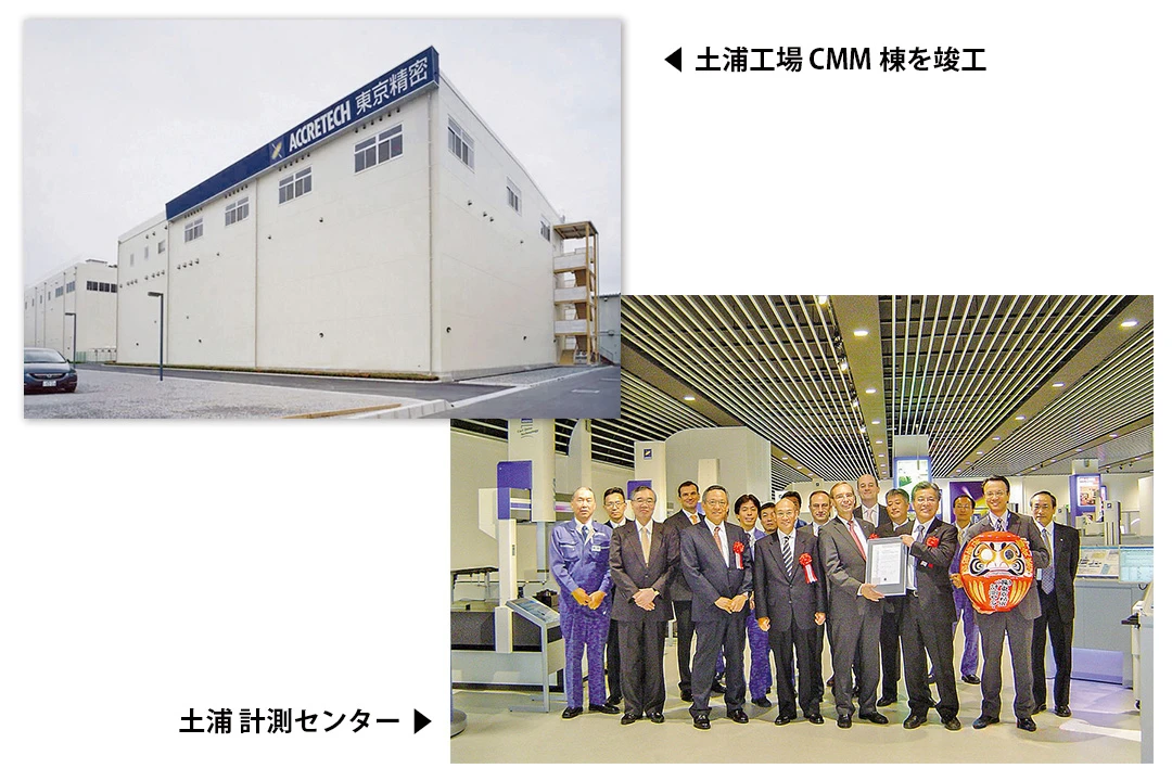
2008
CMM factory completed and Metrology Center opened in Tsuchiura Plant
In response to demand for measuring instruments from a wide range of industries, construction was completed on a CMM building at the Tsuchiura Plant of the Metrology Company. In November of the same year, Metrology Center was opened in the Tsuchiura Plant of the Metrology Company, pushing forward with expansion to strengthen production capacity and application capabilities.
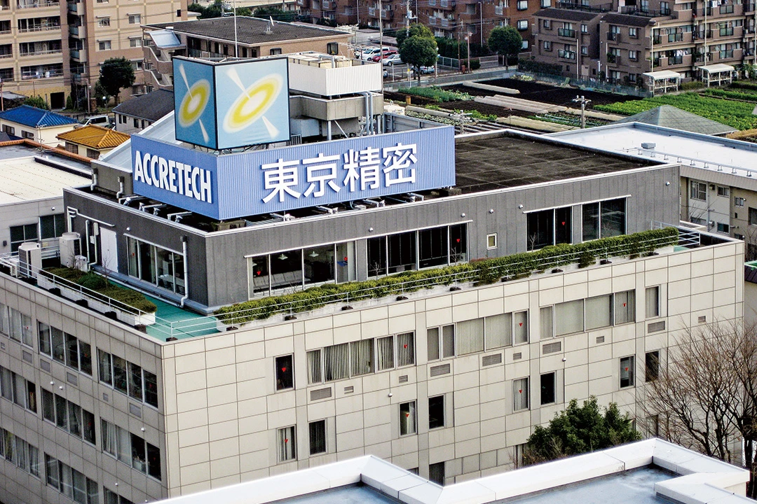
2010
Relocating Head Office from Mitaka
At the end of 2009, Tokyo Seimitsu relocated its Head Office from its birthplace in Mitaka to Hachioji. however, as a consequence of the recessions, the Mitaka Plant was closed and electronics-related production functions were transferred to the Hachioji Plant to be consolidated into the newer functions. In 2009, prior to the closure of the entire Mitaka site, a farewell event was held on its premises, and attendees shared a sea of memories about the site that had accommodated the company’s activities over 60 years.
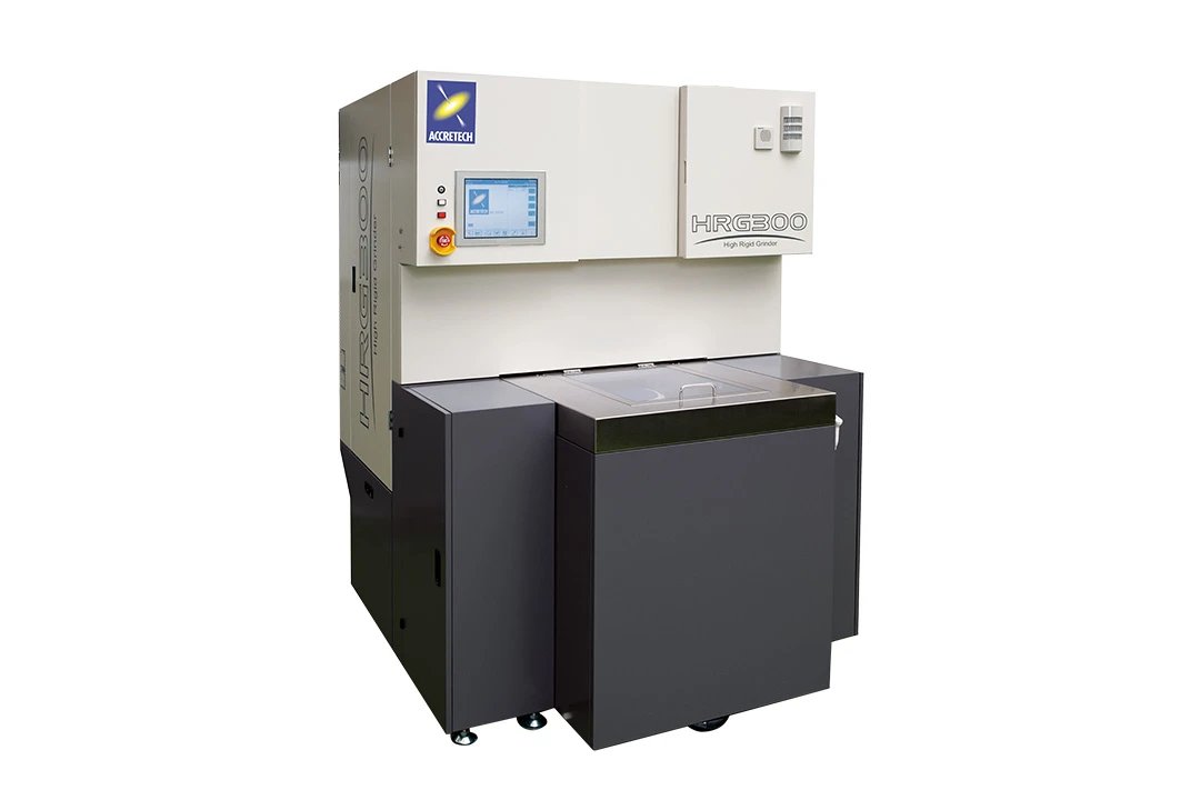
2011
Developed HRG300, high-rigid grinding machine for hard-to-cut material
With growing awareness of the need to save energy and power, and the anticipated full-scale demand for power semiconductors that can minimize electricity waste, we developed a grinding machine for the hard-to-cut materials that will be used to make them. We will contribute to the development of next-generation power semiconductors.
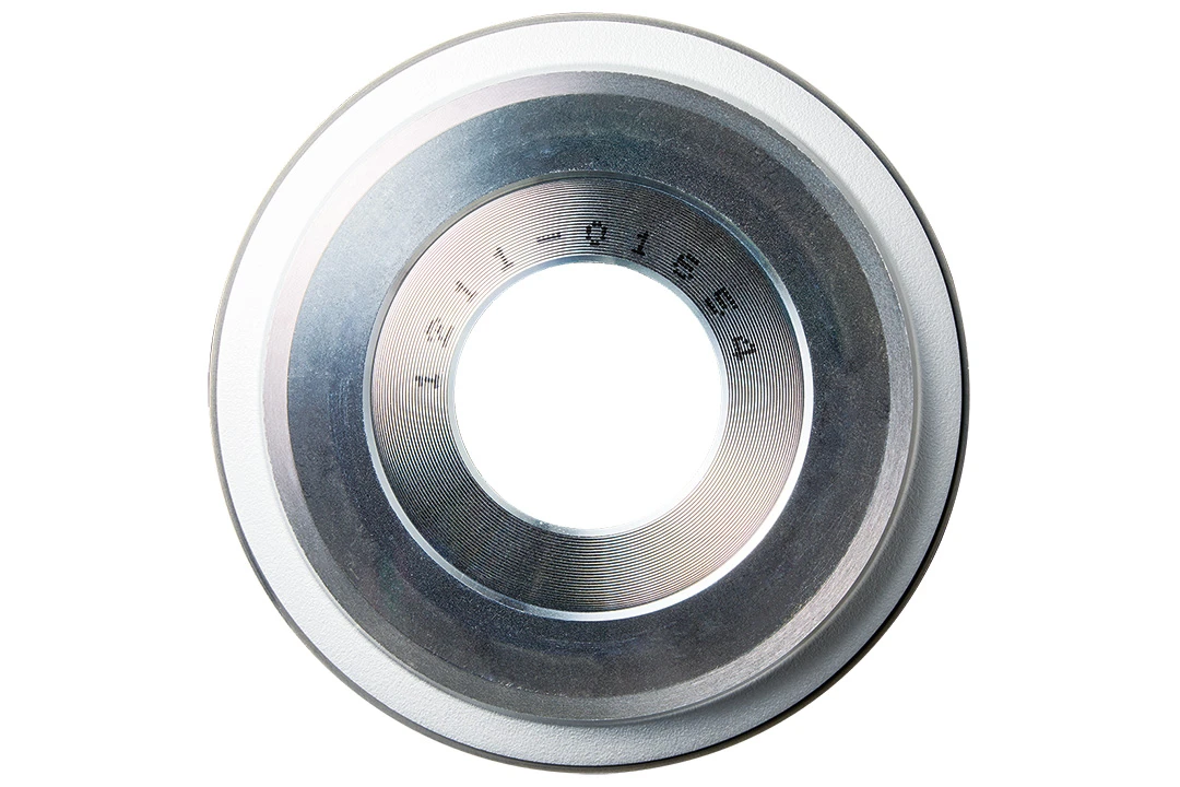
2012
Acquired precision blade business from Mitsubishi Materials Corporation
Promoted mutual cooperation between blades and dicing equipment, dramatically increasing our ability to respond to our customers.
2017
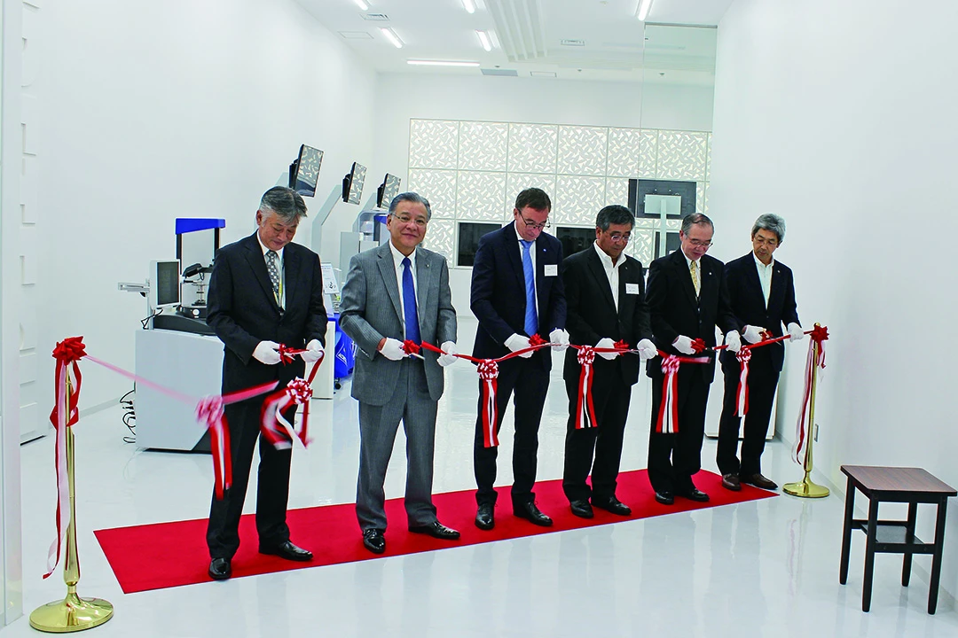
Reopened Metrology Center in Hachioji
The Metrology Center in Hachioji Plant No. 5 was renewed. The space of showroom was expanded to four times larger than before, and the product lineup on display has been enhanced. Training schools and various technical support systems have been strengthened, and the service base in the Kanto area has been enhanced following the showroom in the Tsuchiura Plant.
2019
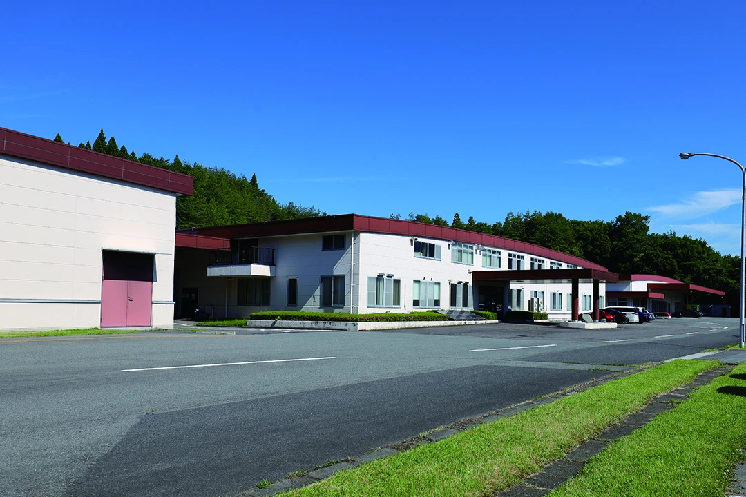
Accretech Powertro Systems started up
Acquired the shares of Fujitsu Telecom Networks Fukushima and started as a subsidiary Accretech Powertronic Systems Co., Ltd. With the dramatic growth in the production of rechargeable batteries expected due to the spread of electric vehicles and the increased introduction of renewable energy, we will contribute to the realization of a sustainable society by supporting research and development and accelerating the spread of rechargeable batteries.
※Business transferred to Tokyo Seimitsu Co. in Oct. 2023.
2020
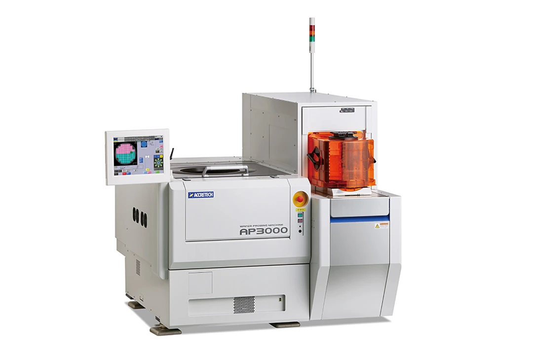
Developed AP3000, wafer probing machine
The technologies required for wafer testing are diverse. Many paradigm shifts are being repeated as they are required to evolve in accordance with the applications and features of the devices to be tested. In particular, the features of today's devices are more pronounced than ever before. In anticipation of next-generation wafer testing trends, we have developed the AP3000/AP3000e to refine flexibility and reliability.
2021
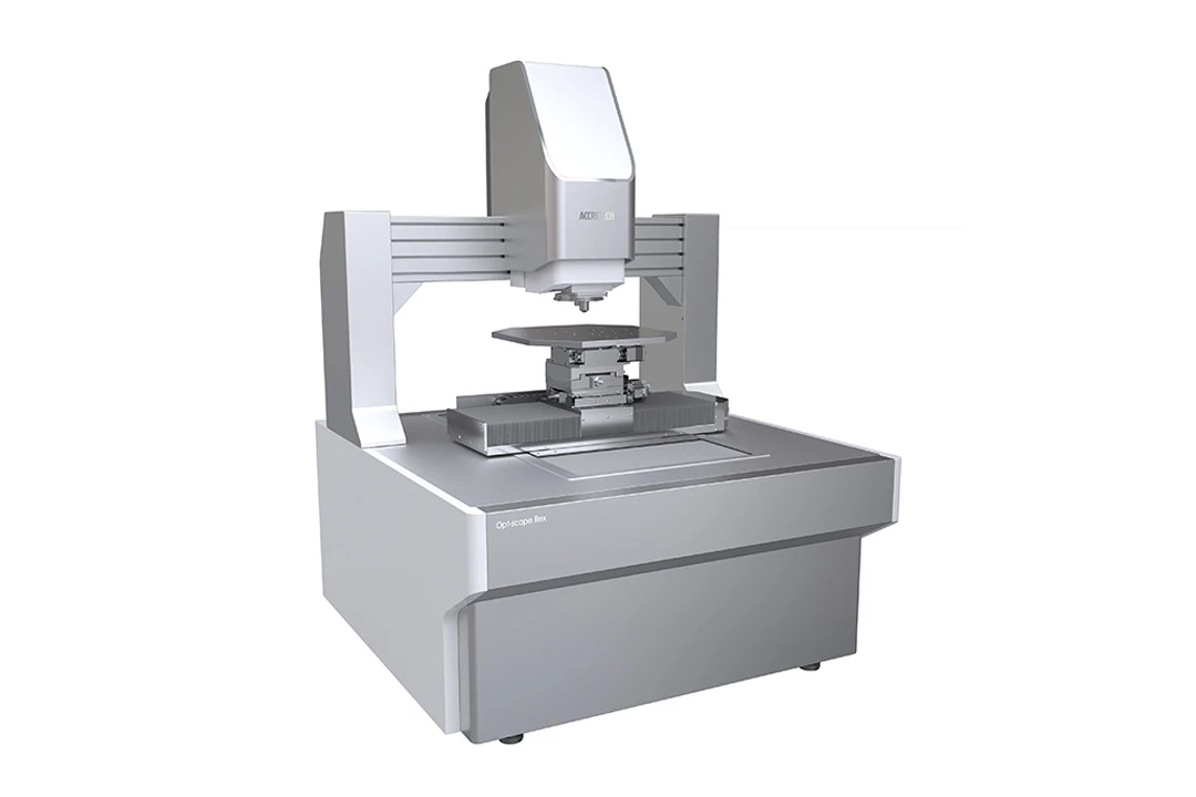
Developed Opt-scope Rex, optical measuring instrument
Opt-scope, which became available in 2015, enables sub-nanometer-level surface roughness measurement, which is impossible with a laser microscope, and is available in a range of work piece sizes.
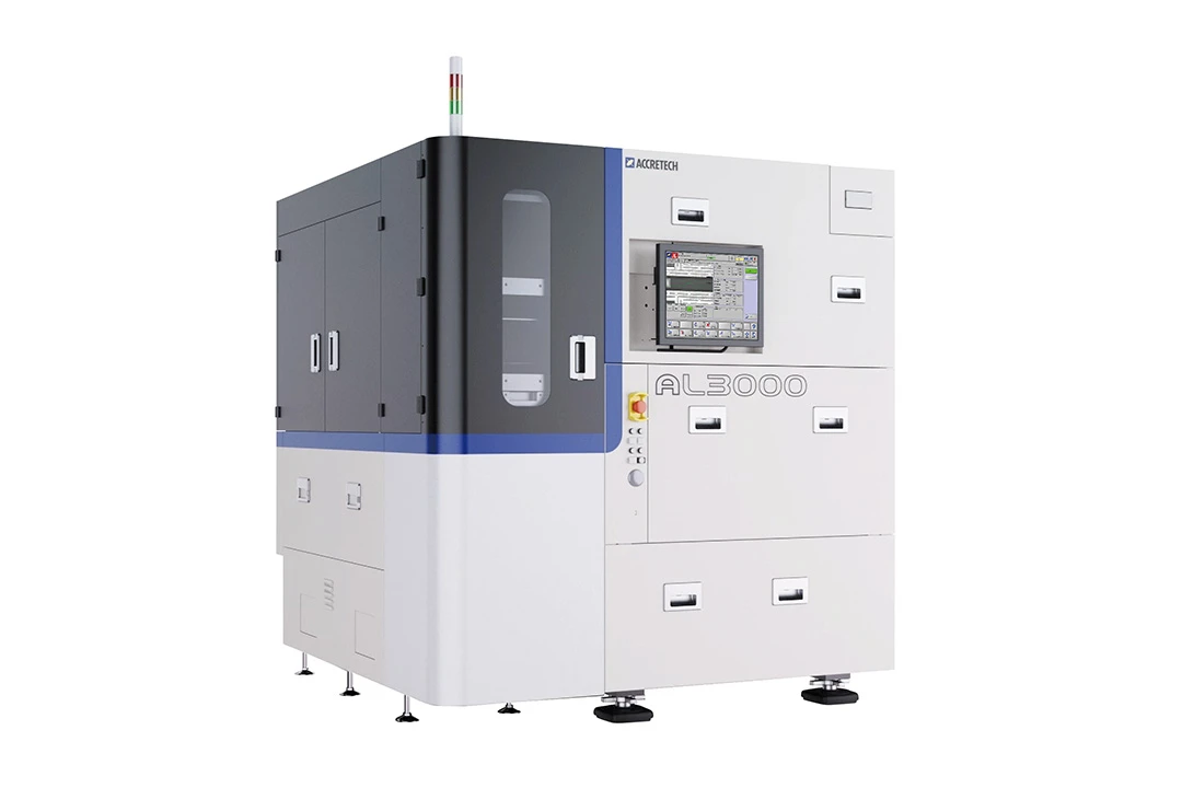
Developed laser dicing machine AL3000
Developed by combining our proprietary laser engine mechanism with a highly rigid, high-precision platform. The AL3000 meets the needs of the market for higher functionality semiconductor devices, higher quality processing, and lower cost.
2023
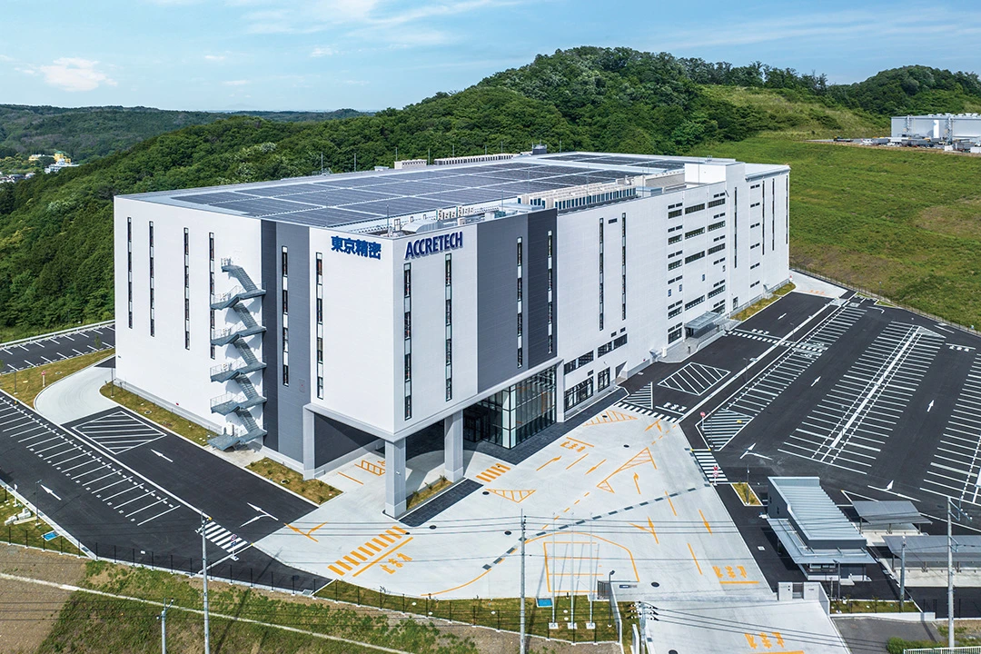
Hanno Plant completed
The completion of the new plant expands our production capacity for semiconductor manufacturing equipment.
2025
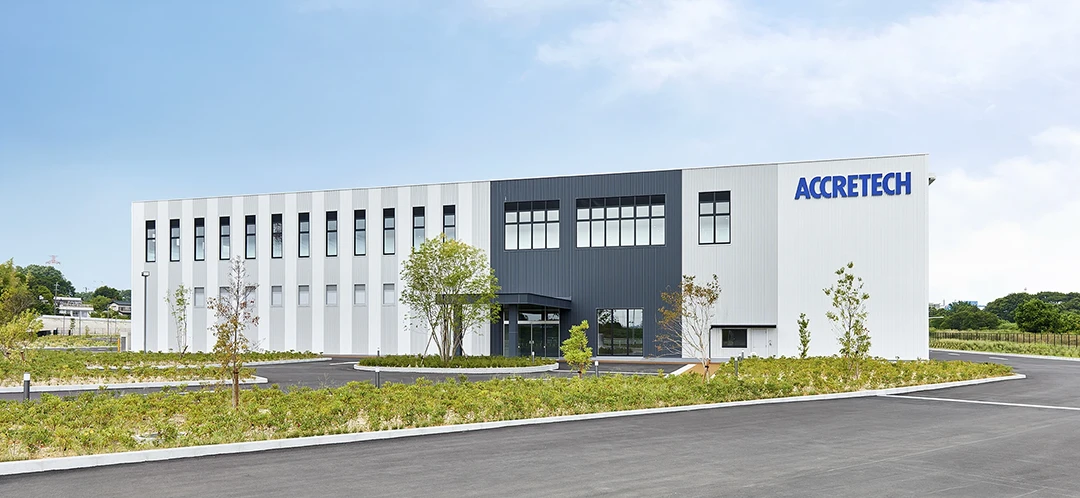
Nagoya Plant of Tosei Engineering Corp. completed
The production capacity for semiconductor manufacturing equipment has been expanded.
Additionally, "Chubu Metrology Center" has been established within the plant as a hub for providing technical support and solutions in precision measurement technology.
*Tosei Engineering Corp. is a group company of Tokyo Seimitsu.
Basic Policies
ACCRETECH Group Code of Conduct

Tokyo Seimitsu Co., Ltd. (here in after referred as “ACCRETECH”) has adopted the basic policy to build WIN-WIN relationships with its customers, shareholders, investors, employees, suppliers, governments, and other stakeholders and together achieve long-term sustainable growth. To this end, ACCRETECH shall do the right thing so that it is well accepted in communities in which it operates.
ACCRETECH Group (ACCRETECH, its subsidiaries and its affiliated companies) established this ACCRETECH Group Code of Conduct (here in after referred as “Code of Conduct”) to provide a set of guiding principles which are to be observed by all directors, auditors and employees of ACCRETECH Group (collectively referred to as “ACCRETECH Officers and Employees”). ACCRETECH Group shall meet the highest ethical standards and establish transparency in management systems to promote compliance.
Through the promotion of education to all ACCRETECH Officers and Employees, ACCRETECH Group shall raise their awareness to observe this Code of Conduct.
ACCRETECH Group shall make sincere efforts to obtain understanding and cooperation from all stakeholders in its compliance activities.
Document Library


