From electronic materials such as semiconductors and electronic components, to semiconductor manufacturing equipment and electronic component manufacturing equipment, it is important to support reliability, reproducibility, and quality in dimensional tolerances, geometric tolerances, and surface roughness in reference design drawings. ACCRETECH will propose optimal solutions for all processes, from development to quality control.
Growing Demand for Precision Measurement
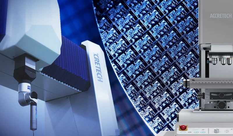
Semiconductors and electronic components are some of the industries most advanced and developed by Japan. With applications ranging from smartphones to super computers, and from flat televisions to autonomous driving, semiconductors and electronic components are core technologies of Industry 4.0 as they contribute to the key focuses of high volume, low power consumption, and high speed. A truly vast number of components are used in related production equipment, from semiconductor and electronic component manufacturing equipment, to vacuum chambers, vacuum pumps, high-purity valves, pipes, electrostatic chucks, and electrodes. Moreover, the reliability, reproducibility, and quality of each of these components relies heavily upon the dimensional tolerance, geometric tolerance, and surface roughness provided on design drawings. Compared to other machinery-related industries, the semiconductor and electronic component industries must stringently control dimensional accuracy and surface roughness, therefore have even higher demands for precision measurement.
Surface roughness affecting the electrostatic adsorption force of an electrostatic chuck (ESC)
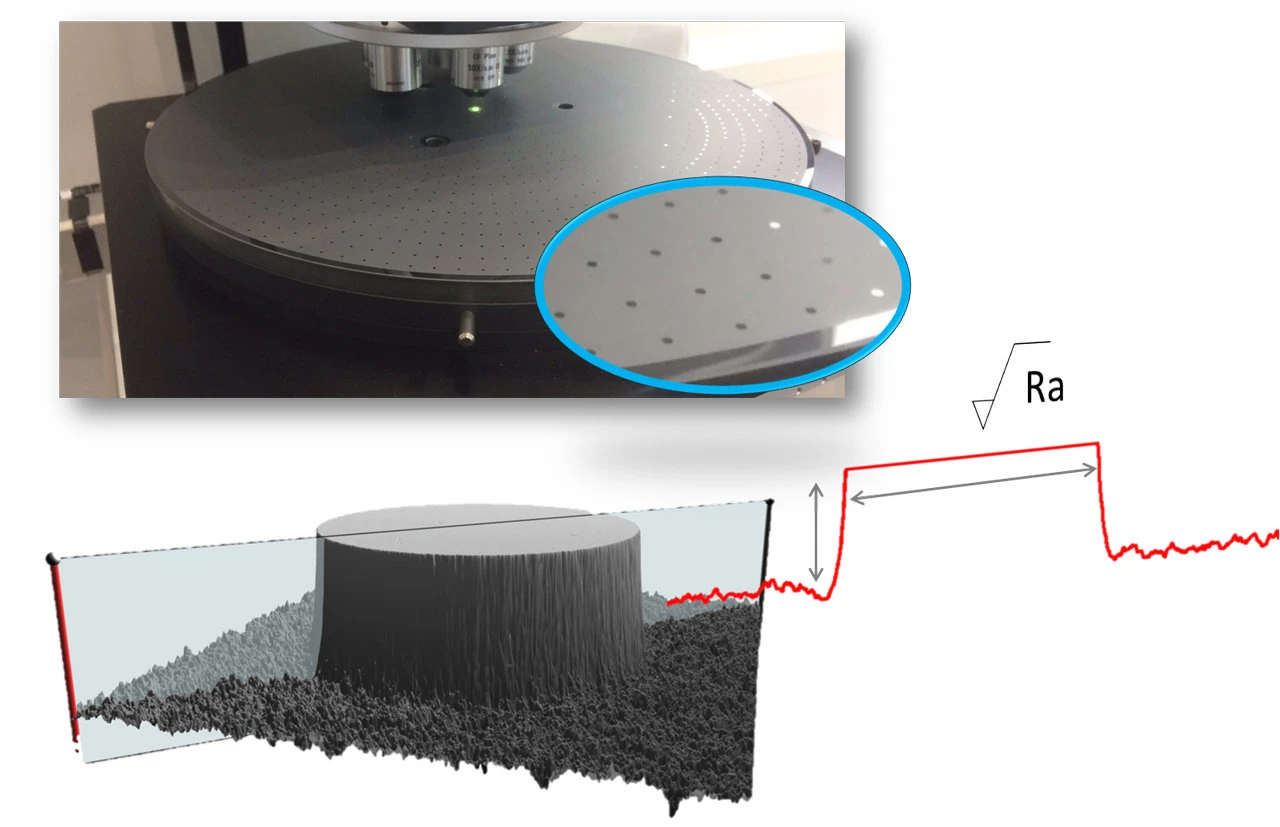
ESCs are used as the electrostatic adsorption mechanism for semiconductor wafers in etching equipment, in the plasma processing equipment that carries out thin film formation by CVD, and other equipment integral to the semiconductor device manufacturing process. In some cases, the adsorption face of the ESC, which holds the wafer using electrostatic adsorption force, is embossed in order to minimize particle adhesion. The roughness of the embossed surface significantly affects the ESC’s adsorption force and thermal control, therefore surface roughness is an important quality control parameter. ACCRETECH proposes both contact and non-contact solutions for controlling surface roughness.
External dimensions, flatness, and parallelism of electrostatic chucks (ESC)
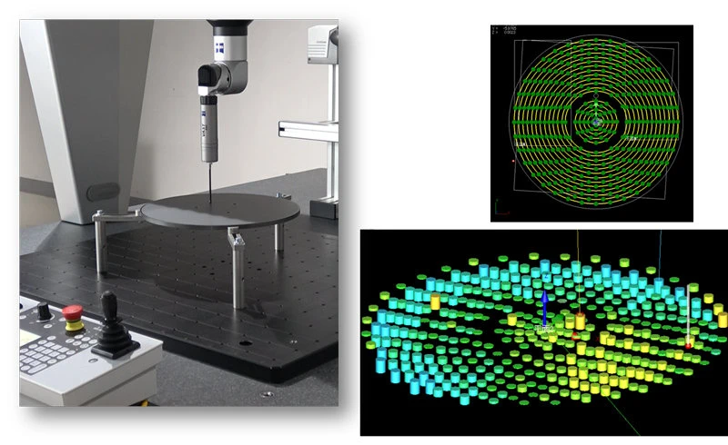
In addition to the surface roughness discussed above, other parameters affecting the electrostatic adsorption force of ESCs, as the electrostatic adsorption mechanism of semiconductor wafers, are external dimensions, as well as the flatness and parallelism of the top and bottom faces. These parameters are also important from the perspective of horizontally securing the wafer being adsorbed to the extent possible. ACCRETECH proposes both contact and non-contact solutions for controlling dimensions and geometric shape.
Dimensional Measurement and Geometric Tolerance Evaluation of Quartz Glass Parts
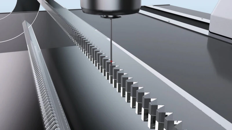
Quartz glass parts are indispensable materials in the processing of semiconductors, which despise contamination, and are often used in semiconductor manufacturing equipment performing processes such as exposure, cleaning, diffusion, deposition, ionization, and etching. Quartz glass parts are used in a wide-range of applications, such as photomasks, quartz chambers in vertical furnaces used for diffusion and deposition, and quartz boats that guide wafers, therefore the processing accuracy required for such parts varies greatly. For example, quartz boats can lead to process abnormalities if the dimensions and shape accuracy of the wafer guide pitch, wafer contact, contact with other components, and fixing parts are not properly managed. As the optimal solution to such issues, ACCRETECH proposes a CMM equipped with a high-precision scanning probe system boasting a solid track record in dimensional measurement and geometric tolerance evaluation.


